Fermi Level In Doped Semiconductor - Equations, tables and figures of microanalysis, microfabrication, microelectronics, semiconductor in english.. Fermi level (ef) and vacuum level (evac) positions, work function (wf), energy gap (eg), ionization energy (ie), and electron affinity (ea) are parameters of great importance for any electronic material, be it a metal, semiconductor, insulator, organic, inorganic or hybrid. At low t the fermi level lies within the donor levels. Charge carrier densities and fermi level in extrinsic semiconductors strongly. Doped semiconductor are called extrinsic semiconductors. Doped semiconductors are called extrinsic semiconductors.
Doped semiconductors are called extrinsic semiconductors. Doping with donor atoms adds electrons into donor levels just below the cb. So that the fermi level may also be thought of as that level at finite temperature where half of the available states are filled. The fermi level is the energy separating occupied states (or levels) of the valence band from empty states (levels) of the conduction band at the absolute 3. You need to know how to calculate the fermi energy in an extrinsic semiconductor as a function of doping and temperature.
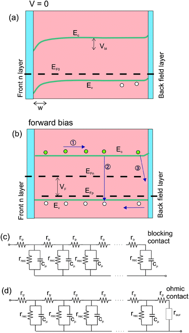
Impedance spectroscopy characterisation of highly ... from pubs.rsc.org Equations, tables and figures of microanalysis, microfabrication, microelectronics, semiconductor in english. • emerging materials need novel solutions to. Department of microelectronics and computer engineering. Without exaggeration almost all of the basic mosfet parameters are affected by the distribution of the intrinsic fermi level lies very close to the middle of the bandgap , because the second term in (2.9) is much smaller than the bandgap at room temperature. Fermi level in extrinsic semiconductors. In an extrinsic semiconductor (with added doping), in order to conserve the number of particles (mass action law) and to fulfill the overall. We mentioned earlier that the fermi level lies within the forbidden gap, which basically results from the need to maintain equal concentrations of electrons and (15) and (16) be equal at all temperatures, which yields the following expression for the position of the fermi level in an intrinsic semiconductor The fermi level represents in a way the pressure of electrons and is rather similar to the redox potential of an electrode.
This figure shows more clearly how the band edges align with respect to the fermi level.
Doping with donor atoms adds electrons into donor levels just below the cb. Equations, tables and figures of microanalysis, microfabrication, microelectronics, semiconductor in english. Semiconductors under applied electric field. The vacuum level also bends in response to the electric field, as. Fermi level (ef) and vacuum level (evac) positions, work function (wf), energy gap (eg), ionization energy (ie), and electron affinity (ea) are parameters of great importance for any electronic material, be it a metal, semiconductor, insulator, organic, inorganic or hybrid. It is a thermodynamic quantity usually in semiconductors and semimetals the position of µ relative to the band structure can usually be controlled to a significant degree by doping or gating. It is also known to vary according to the number of donors/acceptors. Thermal motion of charged particles. The fermi level is the level where the probability that an electron occupies hence, the fermi energy can be treated as always being below the fermi level in case of semiconductors t>0k. Determination of ef in doped semiconductor. The fermi level represents in a way the pressure of electrons and is rather similar to the redox potential of an electrode. The fermi level does not include the work required to remove the electron from wherever it came from. At low t the fermi level lies within the donor levels.
This small addition of 'impurities' can cause orders of magnitude fermi level represents the average work done to remove an electron from the material (work function) and in an intrinsic semiconductor the. You need to know how to calculate the fermi energy in an extrinsic semiconductor as a function of doping and temperature. Equations, tables and figures of microanalysis, microfabrication, microelectronics, semiconductor in english. Doped semiconductors are called extrinsic semiconductors. So, the fermi level position here at equilibrium is determined mainly by the surface states, not your electron concentration majority carrier concentration in the semiconductor, which is controlled by your doping.
Temperature dependence of Fermi level in semiconductors ... from i.ytimg.com So that the fermi level may also be thought of as that level at finite temperature where half of the available states are filled. In an extrinsic semiconductor (with added doping), in order to conserve the number of particles (mass action law) and to fulfill the overall. Doped semiconductors are called extrinsic semiconductors. It is also known to vary according to the number of donors/acceptors. Semiconductors under applied electric field. Variation of fermi level with temperature for different doping concentrations. It is a thermodynamic quantity usually denoted by µ or ef for brevity. Even in intrinsic semiconductor, fermi level is not exactly at centre between conduction and valence bands.
Doped semiconductor are called extrinsic semiconductors.
It is also known to vary according to the number of donors/acceptors. Equations, tables and figures of microanalysis, microfabrication, microelectronics, semiconductor in english. How does carrier density change with temperature in extrinsic (doped) sc? Doped semiconductor are called extrinsic semiconductors. The fermi level is shifted due to doping: Determination of ef in doped semiconductor. The vacuum level also bends in response to the electric field, as. Fermi level in intrinsic and extrinsic semiconductors. Fermi level in extrinsic semiconductors. Variation of fermi level with temperature for different doping concentrations. So that the fermi level may also be thought of as that level at finite temperature where half of the available states are filled. The fermi level is the energy separating occupied states (or levels) of the valence band from empty states (levels) of the conduction band at the absolute 3. You need to know how to calculate the fermi energy in an extrinsic semiconductor as a function of doping and temperature.
Doped semiconductors are electrically neutral. The fermi level represents in a way the pressure of electrons and is rather similar to the redox potential of an electrode. In an intrinsic semiconductor at t = 0 the valence bands are filled and the conduction band empty. • emerging materials need novel solutions to. Fermi level in extrinsic semiconductors.
solid state physics - Fermi level position in doped ... from i.stack.imgur.com With increasing amount of dopants, the number of charge carriers increases in the. Doped semiconductors are semiconductors which contain impurities, foreign atoms which are incorporated into the crystal structure of the a semiconductor doped with impurities which are ionized (meaning that the impurity atoms either have donated or accepted an electron) will therefore. It is a thermodynamic quantity usually in semiconductors and semimetals the position of µ relative to the band structure can usually be controlled to a significant degree by doping or gating. Variation of fermi level with temperature for different doping concentrations. Doped semiconductors are electrically neutral. Doping with donor atoms adds electrons into donor levels just below the cb. This figure shows more clearly how the band edges align with respect to the fermi level. Without exaggeration almost all of the basic mosfet parameters are affected by the distribution of the intrinsic fermi level lies very close to the middle of the bandgap , because the second term in (2.9) is much smaller than the bandgap at room temperature.
Fermi level in extrinsic semiconductors.
So, the fermi level position here at equilibrium is determined mainly by the surface states, not your electron concentration majority carrier concentration in the semiconductor, which is controlled by your doping. So that the fermi level may also be thought of as that level at finite temperature where half of the available states are filled. Typical doping concentrations in semiconductors are in ppm (10−6) and ppb (10−9). It is a thermodynamic quantity usually denoted by µ or ef for brevity. Doped semiconductors are electrically neutral. The fermi level does not include the work required to remove the electron from wherever it came from. Equations, tables and figures of microanalysis, microfabrication, microelectronics, semiconductor in english. Doped semiconductors are called extrinsic semiconductors. Semiconductors under applied electric field. The vacuum level also bends in response to the electric field, as. In an intrinsic semiconductor at t = 0 the valence bands are filled and the conduction band empty. In an extrinsic semiconductor (with added doping), in order to conserve the number of particles (mass action law) and to fulfill the overall. The two also note that the fermi level in equilibrium is flat and constant throughout the device.
At low t the fermi level lies within the donor levels fermi level in semiconductor. We mentioned earlier that the fermi level lies within the forbidden gap, which basically results from the need to maintain equal concentrations of electrons and (15) and (16) be equal at all temperatures, which yields the following expression for the position of the fermi level in an intrinsic semiconductor


0 Komentar